Talks
Rudolf Bratschitsch, U Münster
Single-photon emitters in 2D materials
Graphene is known as a prototypical two-dimensional material with unique physical properties. However, the difficulty of creating an optical band gap stimulated the search for other monolayer materials.
Atomically thin transition metal dichalcogenides serve as a promising new material class for opto-electronics. In contrast to thicker crystals, monolayers of MoS2, WS2, MoSe2, and WSe2 exhibit prominent photoluminescence. Recently, we have discovered bright and stable single-photon emitters in single layers of WSe2 [1], which renders atomically thin semiconductors also interesting for quantum optics. In my talk, I will show that these quantum light sources are strain-induced and demonstrate deterministic positioning of the emitters on the nanoscale [2]. Furthermore, I will present single-photon emission from the layered monochalcogenide semiconductor GaSe [3] and provide evidence that the incorporated non-classical light sources are also strain-induced. Next, I will demonstrate that these single photons originating from GaSe emitters can be routed in dielectric waveguides on a photonic chip [4]. Finally, I will discuss the nature and prospects of newly discovered single-photon emitters in hBN [5].
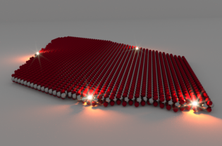
Figure 1:
Artistic impression of a WSe2 monolayer with several single-photon emitters
References:
[1] P. Tonndorf et al., Optica 2, 347 (2015).
[2] J. Kern et al., Advanced Materials 28, 7101 (2016).
[3] P. Tonndorf et al., 2D Materials 4, 021010 (2017).
[4] P. Tonndorf at al., Nano Letters 17, 5446 (2017).
[5] D. Wigger at al., 2D Materials 6, 035006 (2019).
Daniele Brida, U Luxembourg
Attosecond Current Autocorrelations Driven by Single-Cycle Laser Pulses
We performed interferometric autocorrelation measurements with single-cycle pulses that exploit the electric currents coherently driven at the gap of a single nanodevice [1] by optical pulses with pJ energies[2]. The full width at half maximum of the current autocorrelation amounts to less than one femtosecond, demonostrating that we can transfer individual electrons between the two contacts on an attosecond time scale.
In the future, we are aiming at a regime where the Coulomb interaction between electrons becomes important at truly atomic time and length scales.
Figure 1
(a) Conceptual sketch of the experiment with two single-cycle light pulses at delay time Δt focused on the nanogap of the circuit. The carrier-envelope phase of the biasing pulses can selected arbitrarily. (b) Scanning electron micrograph of the nanocircuit employed in the experiments, consisting of an Au optical antenna with electrical leads on a fused-silica substrate. (c) Colormap of nanotunneling current as a function of delay between the two driving pulses and as a function of their carrier-envelope phase. (d) Autocorrelation trace as a function of time delay Δt measured for a carrier-envelope phase of 0 (i.e. cosine-like pulses), corresponding to maximum total current.
References:
[1] T. Rybka, M. Ludwig, M. F. Schmalz, V. Knittel, D. Brida und A. Leitenstorfer, Nature Photon. 10, 667–670 (2016).
[2] D. Brida, G. Krauss, A. Sell and A. Leitenstorfer, Laser Phot. Rev. 8, 409-428 (2014).
Axel Bruchhausen, Centro Atómico Bariloche & Instituto Balseiro (ARG)
Dynamics of inter-layer vibrational modes in 2H-MoSe2 molecular membranes
Dimensionality radically changes the physical properties not only due to the density-of-states effect, but also due to changes in the fundamental interactions that dominate when gradually lowering the size. The family of semiconductor transition metal dichalcogenides (TMDCs) is a specially promising platform for fundamental studies in these kind of uttermost low-dimensional systems. Unlike graphene, TMDCs are optically active, and thus have potential applications in many fields such as optoelectronics, valleytronics, and hybrid optomechanics, due to their direct band-gap in the monolayer limit, together with their highly efficient light-matter coupling [1].
Quantized mechanical vibrations (phonons) play a decisive role in most of these fields and applications, and are thus interesting to be characterized and analyzed.
By means of ultra-fast laser spectroscopy and Raman spectroscopy, we investigate the acoustic phonon dynamics in 2H-MoSe2 as function of the number of piled up molecular layers, and observe a clear change in the acoustic lifetime that is associated to different processes that dominate when going from a 3D to a strictly 2D situation [1]. For thicker samples, the main acoustic attenuation mechanism is attributed to the scattering of the acoustic modes with thermal phonons, while for thinner samples the dominant damping mechanism appears to be ascribed to surface asperity (see Fig.1). In addition, important vibrational and excitonic changes are observed when the systems are supported by a substrate [3].
Figure 1:
Measured lifetime of the interlayer B1-modes as function of their frequency for membranes with different number of layers (L), as indicated. Inset: Derived asperity for the thinnest membranes.
References:
[1] Qing Hua Wang, et al., Nature Nanotechnology 7, 699 (2012).
[2] P. Soubelet, et al., Nanoscale 11, 10446 (2019).
[3] P. Soubelet, et al., in preparation.
J. Carlos Cuevas, UA Madrid (ESP)
Thermal Management in Molecular Junctions
With the advent of novel fabrication techniques in the 1980s and 1990s, it became possible to explore many physical phenomena at the nanoscale. Since then, a lot of progress has been done in the understanding of the electronic transport, mechanical, and optical properties of nanoscale devices. However, thermal transport in these systems has remained relatively unexplored because of the experimental difficulty to measure the flow of heat and energy at this small scale. In this talk, I will review our theoretical and experimental efforts to establish the fundamental laws that govern nanoscale thermal transport by using atomic and molecular junctions as a playground. In particular, I will discuss basic physical phenomena related to the thermal management such as Joule heating [1] and Peltier cooling [2] in molecular junctions.
Figure 1:
Artistic view of a setup to measure Peltier cooling and Joule heating in molecular junctions.
References:
[1] W. Lee, K. Kim, W. Jeong, L.A. Zotti, F. Pauly, J.C. Cuevas, P. Reddy, Nature 498, 209 (2013).
[2] L. Cui, R. Miao, K. Wang, D. Thompson, L.A. Zotti, J.C. Cuevas, E. Meyhofer, P. Reddy, Nature Nanotechnology 13, 122 (2018).
Artur Erbe, HZD Rossendorf
Combining top-down and bottom-up approaches for nanoelectronic devices
Scaling electronic devices to smallest structure sizes well below 10nm will require novel developments for the fabrication of single components. Smallest functional devices can be assembled using chemical methods leading to, e.g., single molecules with electronic functionalities. Reliable contacting of single molecules using metallic contacts is, however, an extremely challenging task which has not been solved so far. We have therefore developed techniques which use self-assembly for the creation of conducting nanostructures in order to create small, self-assembled circuits which then can be contacted reliably using standard lithographic methods.
In this talk, single organic molecules will be presented as active electronic building blocks, which are characterized in mechanically controllable break junctions. In addition, we show how DNA Origamis can be used for the self-assembly of metallic nanowires, which are contacted using electron beam lithography and electrically characterized. Self-assembly can be used for the integration of semiconducting nanoparticles or single molecules for building nanodevices. Further integration of such nanostructures into standard silicon electronics may for example be achieved by connecting these nanodevices to silicon nanowires. We have therefore developed silicon nanowires using electron beam lithography and dry etching (i.e. using a classical top-down approach), which are reconfigurable. With the combination of these wires with self-assembled nanostructures, a large variety of electronic nanocircuits can be constructed in future applications.
Rupert Huber, U Regensburg
The nanoworld in slow motion
A long-standing vision of nanoscience has been to study the microscopic function of condensed matter by directly watching its atomic building blocks dynamically interact on their intrinsic length and time scales. Recently, lightwave electronics has made this long-standing dream come true [1-7]. The idea is to exploit the carrier wave of intense light pulses as an ultrafast, contact-free bias to interrogate and control the nanoworld.
We will first review how lightwaves can drive electrons in solids into surprising quantum motion faster than a cycle of light. Examples range from dynamical Bloch oscillations [2-4] to quasiparticle collisions [5]. In the unique environment of topological insulators, electrons can be accelerated like relativistic particles to cover large distances without scattering and heating [6], moving lightwave-electronic devices into practical reach. Internal quantum attributes of electrons, such as the spin [8,9] or the valley pseudospin [10,11] may be harnessed for potential future quantum information technology, at optical clock rates.
By combining lightwave electronics with the sub-angstrom resolution of scanning tunneling microscopy, we record the first-ever atom-scale slow-motion movies of individual vibrating molecules [12]. The time resolution of our new concept is expected to be widely tunable in the femto- and attosecond regime to visualize structural as well as electronic charge and spin dynamics in ultrafast videography. Finally, I will show how to directly exert femtosecond atomic forces, which can selectively choreograph a coherent structural motion of a single-molecule switch in its electronic ground state [13]. This stunningly direct access to the atomic world may tailor key elementary dynamics in nature and steer (bio)chemical reactions or ultrafast phase transitions, on their intrinsic spatio-temporal scales.
Figure 1:
Femtosecond atomic forces can prepare a structural wavepacket motion of a single-molecule switch (Mg phthalocyanine on NaCl), which coherently controls the switching process.
[1] P. B. Corkum and F. Krausz, Nature Physics 3, 381 (2007), and references therein.
[2] O. Schubert et al., Nature Photonics 8, 119 (2014).
[3] M. Hohenleutner et al., Nature 523, 572 (2015).
[4] F. Langer et al., Nature Photonics 11, 227 (2017).
[5] F. Langer et al., Nature 533, 225 (2016).
[6] J. Reimann et al., Nature 562, 396 (2018).
[7] C. Schmidt et al., Nature Communications 9, 2890 (2018).
[8] S. Baierl et al., Nature Photonics 10, 715 (2016).
[9] S. Schlauderer et al., Nature 569, 383 (2019).
[10] F. Langer et al., Nature 557, 76 (2018).
[11] P. Merkl et al., Nature Materials 18, 691 (2019).
[12] T. L. Cocker, D. Peller et al., Nature 539, 263 (2016).
[13] D. Peller et al., under review.
Mathias Kläui, U Mainz
Topological spintronics devices for GreenIT
In our information-everywhere society IT is a major player for energy consumption. Novel spintronic devices can play a role in the quest for GreenIT if they are stable and can transport and manipulate spin with low power. Devices have been proposed, where switching by energy-efficient approaches, such as spin-polarized currents is used [1], for which we develop new highly spin-polarized materials and characterize the spin transport using THz spectroscopy [2].
Firstly, to obtain ultimate stability of states, topological spin structures that emerge due to the Dzyaloshinskii-Moriya interaction (DMI) at structurally asymmetric interfaces, such as chiral domain walls and skyrmions with enhanced topological protection can be used [3-5]. We have investigated in detail their dynamics and find that it is governed by the topology of their spin structures [3]. By designing the materials, we can even obtain a skyrmion lattice phase as the ground state [4].
Secondly, for ultimately efficient spin manipulation, we use spin-orbit torques, that can transfer more than 1ħ per electron by transferring not only spin but also orbital angular momentum. We combine ultimately stable skyrmions with spin orbit torques into a skyrmion racetrack device [4], where the real time imaging of the trajectories allows us to quantify the novel skyrmion Hall effect [5]. We furthermore use spin-orbit torque induced skyrmion dynamics for non-conventional stochastic computing applications, where we have developed a skyrmion reshuffler device [6].
Finally, to obtain efficient spin transport, we study graphene and low damping ferro- and antiferromagnetic insulators as spin conduits. We find very long distance spin transport in the diffusive regime [7] and study coherent superfluid transport [8] that can be controlled in a magnon transistor [9].
Figure 1:
Spin transport in a heterostructure visualized.
References:
[1] Review: K. Everschor-Sitte et al., J. Appl. Phys. 124, 240901 (2018).
[2] Z. Jin et al., Nature Phys. 11, 761 (2015).
[3] F. Büttner et al., Nature Phys. 11, 225 (2015).
[4] S. Woo et al, Nature Mater. 15, 501 (2016).
[5] K. Litzius et al., Nature Phys. 13, 170 (2017).
[6] J. Zazvorka et al., Nature Nano. 14, 658 (2019).
[7] R. Lebrun et al., Nature 561, 222 (2018).
[8] Y. Tserkovnyak et al., Phys. Rev. Lett. 119, 187705 (2017).
[9] J. Cramer et al., Nature Commun. 9, 1089 (2018).
Andrey S. Moskalenko, KAIST (KOR)
Time-domain approach to ultrafast quantum optics
The quantum nature of light possesses many astonishing properties rendering it a promising candidate for novel spectroscopy methods of complex many body phenomena, quantum information processing and quantum metrology. Usually such light is characterized in the frequency domain whereas even for broadband quantum states a quasi-continuous-wave picture with a well-defined carrier frequency is still applicable. An alternative approach, especially suitable for the ultrabroadband case, would be to consider the quantum fields directly in the time domain. Technically, this approach can be based on a quantum version of the electro-optic sampling technique [1,2,3]. With this method the quantum electric-field fluctuations of the bare vacuum state [1] and of few-cycle squeezed vacuum states [4] can be detected. Furthermore, corresponding correlation measurements providing information on spectral characteristics of the probed fluctuations can be performed [3,5]. The technique provides a way to resolve the temporal profile of the variance of the probed quantum field with subcycle resolution [2,4], whereas undesired measurement back-action on this field can be effectively avoided.
It is possible to formulate a consistent time-domain theory of the generation and time-resolved detection of few-cycle and down to subcycle pulsed squeezed states, where the quasi-monochromatic picture is not valid anymore. There is a relativistic interpretation of the squeezing process in terms of induced changes in the local flow of time [6]. The time-domain picture can be connected to an ultrabroadband generalized Bogoliubov transformation of creation/annihilation operators [6], leading to spectral properties related to the Unruh-Davies effect with a finite time of acceleration [7]. We find that the conventionally observed asymmetry between squeezing and more pronounced anti-squeezing in the temporal noise traces, resulting from the product character of the Heisenberg’s uncertainty relation, can be reversed in the studied ultrabroadband case. The theory also paves a way for quantum tomography with subcycle temporal resolution.
References:
[1] C. Riek et al., Science 350, 420 (2015)
[2] A.S. Moskalenko et al., Phys. Rev. Lett. 115, 263601 (2015)
[3] I.-C. Benea-Chelmus et al., Nature 568, 202 (2019)
[4] C. Riek et al., Nature 541, 376 (2017)
[5] A.S. Moskalenko and T.C. Ralph, Nature 568, 178 (2019)
[6] M. Kizmann et al., Nat. Phys. 15, 960 (2019)
[7] T.L.M. Guedes et al., Phys. Rev. Lett. 122, 053604 (2019).
Abraham Nitzan, U Pennsylvania (USA) / U Tel Aviv (ISR)
Electron transfer across thermal gradients
Recent advances in observing and manipulating charge and heat transport at the nanoscale, and recently developed techniques for monitoring temperature at high temporal and spatial resolution, imply the need for considering electron transfer across thermal gradients. Here, a theory is developed for the rate of electron transfer and the associated heat transport between donor-acceptor pairs located at sites of different temperatures. The electron transfer rate is obtained as a Marcus-type expression with an effective temperature in which the temperatures of the two sites are weighted by the corresponding reorganization (or small polaron formation) energies. The energy transferred per electron transfer event is calculated and the resulting contribution to the heat conductivity in a system where electronic transport is dominated by electron hopping between polaronic sites is evaluated. Furthermore in a system with three or more sites this kinetics is shown to lead to thermal transistor effects, steady states characterized by circular electronic currents and to rectification of thermoelectric response.
Fabian Pauly, OIST, Okinawa & U Konstanz
Mechanical control of charge and heat transport through nanocontacts
The coupling of electronic and nuclear degrees of freedom plays a decisive role in quantum transport through nanostructures. Vibrations lead to inelastic signals in electrical current and shot noise, they activate hopping transport or cause dephasing. Also, the strain state of a single-molecule junctions can be used to tune charge and heat flows significantly.
I will start with a beautiful example, showing that the conductance of a spring-like molecule can be mechanically controlled by several orders of magnitude by compressing or elongating it [1]. Ab-initio calculations indicate that the large conductance variations are the result of destructive quantum interference effects between the frontier orbitals that can be lifted by applying either compressive or tensile strain to the molecule. The mechanical control of quantum interference effects results in the largest-gauge factor reported for single-molecule devices so far, which may open the door for applications in a nanoscale mechanosensitive sensing device that is functional even at room temperature.
Turning to energy transport, I will present recent experiments that determined the thermal conductance of single-atom and single-molecule contacts for the first time [2,3]. I will explain our present theoretical understanding in terms of the variability of the heat transport with junction structure and the externally controlled strain state [2-5]. New theoretical insights are furthermore gained by an analysis in terms of phononic transmission eigenchannels [6]. By adapting a related method for determining scattering states in fermionic electron systems to the bosonic phonon problem, the one-dimensional nature of the atomic and molecular wires is revealed through a characteristic number of less than three transmissive eigenchannels, and center of mass modes are shown to be crucial for transfer of heat between soft metal electrodes via a stiff carbon-based molecule.
Figure 1:
Heat transport through a single molecule connected between a hot tip and a cold substrate of a scanning tunneling microscope.
References:
[1] D. Stefani, K. J. Weiland, M. Skripnik, C. Hsu, M. L. Perrin, M. Neuburger, M. Mayor, F. Pauly and H. S. J. van der Zant, Nano Lett. 18, 5981 (2018).
[2] L. Cui, W. Jeong, S. Hur, M. Matt, J. C. Klöckner, F. Pauly, P. Nielaba, J. C. Cuevas, E. Meyhofer, and P. Reddy, Science 355, 1192 (2017).
[3] L. Cui, S. Hur, Z. A. Akbar, J. C. Klöckner, W. Jeong, F. Pauly, S.-Y. Jang, P. Reddy, and E. Meyhofer, Nature 572, 628 (2019).
[4] J. C. Klöckner, M. Matt, P. Nielaba, F. Pauly, and J. C. Cuevas, Phys. Rev. B 96, 205405 (2017).
[5] J. C. Klöckner and F. Pauly, arXiv:1910.02443.
[6] J. C. Klöckner, J. C. Cuevas, and F. Pauly, Phys. Rev. B 97, 155432 (2018).
Gianluca Rastelli, U Konstanz
Electron-vibration and electron-photon interaction in quantum dots: towards a mesoscopic QED
Quantum nanoscale conductors coupled to localized resonators such as microwave photon cavities or nanomechanical devices have become commonly studied systems.
Quantum conductors show interesting and unique physics such as spin-dependent transport and nonlocal quantum correlations. Combining them with resonators adds a new dimension to cavity and circuit electrodynamics, beyond the usual paradigm of a single (artificial) atom coupled to a harmonic oscillator.
They open the path to the exploration of the correlations between the charge transport and the nonequilibrium, eventually quantum, regime of the localized resonators. For example, electromechanical systems display a variety of interesting phenomena such as nonlinear dynamical effects induced by the electron transport or the crossover from classical to quantum behaviour of the resonator itself, a massive object formed by millions of atoms. As another example, I show that quantum dots can operate as electrically tunable single atom lasers when they are coupled to microwave cavities.
Finally, I will present a few promising research directions and open challenges of this emerging field.
Ulrike Ritzmann, FU Berlin
Trochoidal motion and pair generation in skyrmion and antiskyrmion dynamics driven by spin-orbit torques
Skyrmions and antiskyrmions can be stabilized in ultrathin magnetic films due to competing interactions as Dzyaloshinskii-Moriya interaction (DMI) and exchange interaction beyond the nearest neighbor approach. They are characterized by opposite topological charges, which govern the sense of gyration in their dynamics. Until now, the robustness of the symmetry between opposite topological charges has not been examined in detail. In particular, the roles of core deformation, the internal degrees of freedom, and the underlying symmetry of the magnetic interactions remain an open question.
We used atomistic spin dynamics simulations with parameters derived from DFT, reduced variable modeling, and machine learning algorithms to study skyrmion and antiskyrmion dynamics under spin-orbit torques. While skyrmions move rectilinear as, we discover new dynamical regimes involving antiskyrmions: trochoidal motion and skyrmion-antiskyrmion pair generation due to core deformations of the antiskyrmion. When a DMI symmetry is chosen that favors antiskyrmions over skyrmions, the opposite behavior is found — antiskyrmions follow rectilinear paths, while skyrmions undergo trochoidal motion and can generate skyrmion-antiskyrmion pairs. This illustrates the importance of the symmetry of the DMI, rather than the topological charge, in governing the dynamics.
Furthermore, we discuss how a skyrmion gas can be generated through the trochoidal motion of an initial antiskyrmion seed [1]. During this trochoidal motion, a skyrmion–antiskyrmion pair is nucleated from the deformed core, much in the same way as a vortex–antivortex pair being nucleated prior to vortex core reversal. In contrast to the vortex core case, the skyrmion–antiskyrmion pair separates because skyrmions and antiskyrmions execute different motion under these torques. Skyrmions readily propagate away from the region of generation through linear motion, while the trochoidal motion of antiskyrmions mean they remain more localized to the generation region. Increased scattering between antiskyrmions leads to annihilation, which results in an overall excess of skyrmions in the system. We investigated how the generation rate and the skyrmion excess depend on the spin-orbit torque parameters. These results provide insight into how skyrmion ensembles may be created in realistic materials.
References:
[1] U. Ritzmann, et al., Nature Electronics 1, 451 (2018).
Uta Schlickum, TU Braunschweig & MPI-Stuttgart
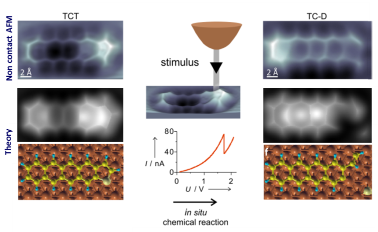
High resolution characterization of surface products
Molecular systems carry intriguing intrinsic functionalities that often come along with complex and dynamic structures. Here, we present high resolution characterization of chemical reactions revealing structural details of reactants and products.
Different ways of chemical reaction paths are explored. We can trigger a direct desulfurization reaction locally on a single molecular unit by the electric field confined in the tunnel junction of a scanning tunnelling microscope [1]. We have also studied Reichardt’s dye molecules that undergo fragmentation reactions on a Cu surface, either by thermal treatment, or after an impact in the hyperthermal energy regime (5-100 eV) during the Electro Spray Ion Beam Deposition (ES-IBD) [2]. For these molecules our analysis demonstrates a reaction mechanism in which the kinetic energy of the collision directly drives the reaction. As a consequence we observe products that cannot be reached through thermal routes, which makes ES-IBD a unique tool for novel chemistry. Surfaces with locally varying reactivity pave the way for further investigations of chemical reactions. Here, we present a way to create h-BN/graphene nano-flake heterostructures on Rh(0001), in which the graphene nanoflakes locally modify the electronic properties of h-BN and with this in line the local reactivity of the surface. This is demonstrated by modified preferred adsorption positions of organic molecules.
References:
[1] B. Borca, T. Michnowicz, R. Pétuya, M. Pristl, V. Schendel, I. Pentegov, U. Kraft, H. Klauk, P. Wahl, R. Gutzler, A. Arnau, U. Schlickum, and K. Kern, Electric field driven direct desulfurization, ACS Nano 11, 4703 (2017).
[2] S. Rauschenbach, M. Ternes, L. Harnau & K. Kern, Mass Spectrometry as a Preparative Tool for the Surface Science of Large Molecules, Annu. Rev. Anal. Chem. 9, 16.1–16.26 (2016).
Denis Seletskiy, Polytechnique Montréal (CAN)
Precise characterization and ultrafast control of electronic spin in single quantum dots
One day, quantum information processing technology is bound to run into bandwidth limitations, similar to those on the side of the classical analogs. Beyond technological outlook, ultrafast quantum light holds a great promise for advancing our understanding of quantum matter on its intrinsic timescales. Novel time-domain quantum states can be achieved through controlled interaction of femtosecond optical pulses with few-charge configurations in single quantum dots. Such spin-photon interfaces are particularly attractive in II-VI semiconductor quantum dots.
Following a detailed study of the electronic structure of singly-charged CdSe/ZnSe quantum dots, we demonstrated their operation as single-photon adders can be initialized on a few picosecond timescales, opening possibilities for ultrafast quantum amplification schemes. After the investigation of the elementary charge dynamics in these systems, we also showed that robust long-lived intraband coherence set up by a femtosecond initialization pulse can be stored and coherently retrieved for up to 100 picoseconds. These experimental findings are enabled by the precise engineering of the femtosecond fiber sources, which will also be outlined in the talk.
In parallel efforts, we advanced epitaxial quantum dots toward fully nano-optimized quantum spin-photon systems. Toward this, through a series of optical studies, we proved that synthesized CdSe/CdS colloidal nanocrystals can be vibrationally decoupled from the substrate by their encapsulation into a nanometer-sized PMMA shell. In particular, the dark character of the exciton can be altered when the bright-dark splitting is brought on resonance with certain confined acoustic phonon modes. Furthermore, by coupling the exciton doublet of the CdSe/CdS/PMMA nanostructures with the plasmonic resonance of a bullseye antenna, we have shown that the total optical emission from the doublet can be enhanced. As part of the ongoing work, we demonstrate an all-optical technique for the determination of the three-dimensional alignment of the colloidal quantum dots. This result will prove important for the upcoming ultrafast coherent control experiments using the newly-developed colloidal quantum dots, which are deterministically charged via functionalization with polyfluorene donors.
Markus Ternes, RWTH Aachen & FZ Jülich
Sensing dark spins with a scanning tunneling microscope
Probing the spin of individual atoms and molecules on surfaces by means of inelastic electron tunneling spectroscopy (IETS) has since its introduction [1] developed to a very successful and widely used method in scanning tunneling microscopy [2]. Recently, IETS measurements have been also taken simultaneously on two magnetic impurities, one attached to the apex at the tip, the other one on the sample surface, revealing correlation-driven transport asymmetries, reminiscent of spin-polarized transport in a magnetic field [3]. In this experiment only the spin on the surface was spectroscopically active while the one on the tip was spectroscopically dark.
Here now I will show how the transport is significantly altered when the tunneling electron is interacting with both spins simultaneously; the one on sample and the one on the tip apex. Different to measurements on two S = 1spins which only showed the expected steps in the differential conductance at each individual excitation and the sum of both excitations [4] we observe complex IETS data when we use a functionalized tip apex with a high S = 3/2 Kondo system to probe a S = 2 Fe adatom on the CuN surface. To successfully simulate such spectrum, Kondo as well as potential scattering processes have to be taken into account whereby strong interference effects due to the fermionic nature of the tunneling electrons lead to novel selection rules [5].
The understanding of the transport rules is important because it enables one to use well understood surface supported spins to calibrate the spin at the ill defined tip apex. Successively, such spin can then be used as a well characterized mobile sensor with unprecedented spacial resolution [6].
References:
[1] A.J. Heinrich, J.A. Gupta, C.P. Lutz, and D.M. Eigler, Science 306, 466 (2004).
[2] M. Ternes, New J. Phys. 17, 063016 (2015).
[3] M. Muenks, P. Jacobson, M. Ternes, and K. Kern, Nature Comm. 8, 14119 (2017).
[4] M. Ormaza, et al., Nano Lett. 17, 1877 (2017).
[5] M. Ternes, C.P. Lutz, A.J. Heinrich, and W.-D. Schneider, arXiv:1908.08267 [cond-mat.mes-hall].
[6] B. Verlhac, et al., accepted for publication in Science (2019).
Peter Wahl, U St. Andrew (UK)
Quantum Criticality in Condensed Matter Physics: An atomic-scale view from model systems to quantum materials
Quantum materials host many properties, which are highly desirable for technological applications, yet our lack of understanding of their physics often prevents them from being exploited. A delicate balance between different competing interactions results in close proximity of emergent orders such as magnetic order and superconductivity and quantum critical behaviour. Understanding the interactions which govern these phases is believed to be key to unravelling their enigmatic properties and making them amenable for applications.
In my talk, I will discuss how we can use low temperature scanning tunnelling microscopy and spectroscopy to gain a better understanding of the microscopic physics in these materials, using atomic-scale model systems (Fig. 1a) [1] as well as spin-polarized scanning tunnelling microscopy [2] to image emergent properties of quantum materials (Fig. 1b) as well as the relation between competing phases [3] .
Figure 1:
(a) Atomic scale model system for quantum criticality [1]. (b) Spin-polarized imaging of the magnetic order in the parent compound Fe1+δTe of the iron chalcogenide superconductors.
References:
1. J. Bork, et al., A tunable two-impurity Kondo system in an atomic point contact, Nat. Phys. 7, 901 (2011).
2. M. Enayat, et al., Real Space Imaging of the Atomic-Scale Magnetic Structure of Fe1+yTe, Science 345, 653 (2014).
3. Ramakrishna Aluru, et al., Atomic-scale coexistence of short-range magnetic order and superconductivity in Fe1+ySe0.1Te0.9, Phys. Rev. Mat. 3, 084805 (2019).